![[NT-MDT: Molecular Devices and Tools for NanoTechnology]](label/ntmdt.gif)
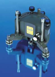
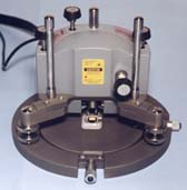
The device intended for complex researches of samples by multi-mode scanning probe microscopy methods.
Plainly place the Stand Alone SMENA on the sample surface of any size and scan the area of interest.
 |
Technical specification: |
|
Accuracy of frequency setting: Digital 32 bit (0.01Hz). Positioning: Manual X,Y positioning stage (range of positioning 6 mm), positioning accuracy 5 um. |
| SMENA - A | SMENA - B | SMENA - C | ||
| COMPLETE Stand Alone system. Combination of SMENA C + SMENA B measuring features with further upgrade to: Spreading Resistance Imaging/ SCM/ SKM/ voltage lithography provides customer with the COMPLETE set of SPM measuring techniques and make it easily upgradeable to FULLY CONFIGURED Solver-P47H multi-mode Universal Scanning probe microscope. SNOM measuring head is available as an option. | middle class Stand Alone system. The upgrade basic model supplies you in addition to SMENA C measuring possibilities with advanced modes such as ResonantMode AFM with RMS + synchronous detection of amplitude and phase up to 9 harmonics for feedback control, Phase Imaging/ MFM/ EFM. | is all you need to start in modern SPM science. The basic model supplies you with modern measuring modes such as ResonantMode (RMS feedback), low sensetive MFM, Force Modulation (viscoelastisity), RM lithography, Contact (Normal and Lateral Force) AFM modes, Adhesion Force Imaging. |
• Polymer investigations • Biological and medical sciences (in combination with Inverse Optical Microscope) semiconductor structures • Magnetic materials • DVD and CD discs • Material investigations • Cars polishing control • Turbine blades • Surface control of Large Optics • etc... |
 Scan size: 10x10 um |
• Stand Alone Scanning probe microscope SMENA is available in 3 configurations: SMENA C, SMENA B, SMENA A. Choose any one based on your application and budget requirements. • UNLIMITED SAMPLE SIZE. Plainly place the Stand Alone SMENA on the sample surface of any size and scan the area of interest. • Extreme resolution. |
 Scan size: 16x16 um |
| The rigid and very light construction of the microscope provides high frequency mechanical loop properties which allows to visualize atomic steps on plane structures even with the use of 30 um scanners (additional vibration isolation required). • All in one (SMENA A): Contact AFM/ LFM/ Adhesion Force Imaging; ResonantModeTM AFM (TappingModeTM + Non-contact mode)/ Phase Imaging/ Force Modulation MFM/ EFM/ SCM/ SKM (SPoM)/ Spreading Resistance Imaging; RM Lithography (Nano Lithography/voltage lithography). • The topography of the same area can be shown simultaneously with LFM/ MFM/ EFM/etc. images for comparison purposes.
• High precision Adhesion Force Microscopy. |
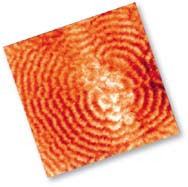
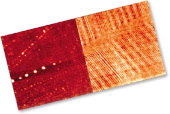 Magnetic force imaging (right). Scan size: 11x11µm) |
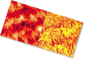 on the left image, phase on the right image. Scan size: 11x11 um) |
Exactly the Snap Back point is measured, so the exact value of force when the snap back happened is registered. • RM (ResonantMode) Lithography performed by mask. • Titanium and compact construction provides low weight (measuring head 0.7kg., electronics block 13kg.) • Wide range of voltage operation 80-250V, 50-60 Hz allows do not care about voltage stabilization. • Low power consumption - 60 W.
• Stand Alone Scanning Probe Microscope SMENA can be extended to a complete Solver-P47H system by ordering additional compounds. |
| The results have been obtained by Dr. Victor Bykov and Dr. Sergei Magonov using Digital Instruments standard samples (polyethylene and DI magnetic test). |
|